 AMD, Apple, MediaTek, Nvidia and Qualcomm are using TSMC’s new manufacturing technologies to produce their new semiconductor chips. While some also use Samsung Foundry to make their chips, these are generally not for high-end products. Samsung Foundry was hoping some would switch to its process instead of TSMC, but that doesn’t look like it’s going to happen anytime soon.
Giants are at TSMC’s door
It was said that Qualcomm could use both Samsung Foundry and TSMC’s 3nm processes for Snapdragon 8 Gen 4 in 2024. However, a new report from China Times claims that both MediaTek and Qualcomm are planning to use TSMC’s second generation 3nm process (N3E) to produce Dimensity 9400 and Snapdragon 8 Gen 4. This new technology offers performance and efficiency improvements over the N3B (first-generation 3nm) process that Apple currently uses to make the A17 Pro processor for the iPhone 15 Pro series.
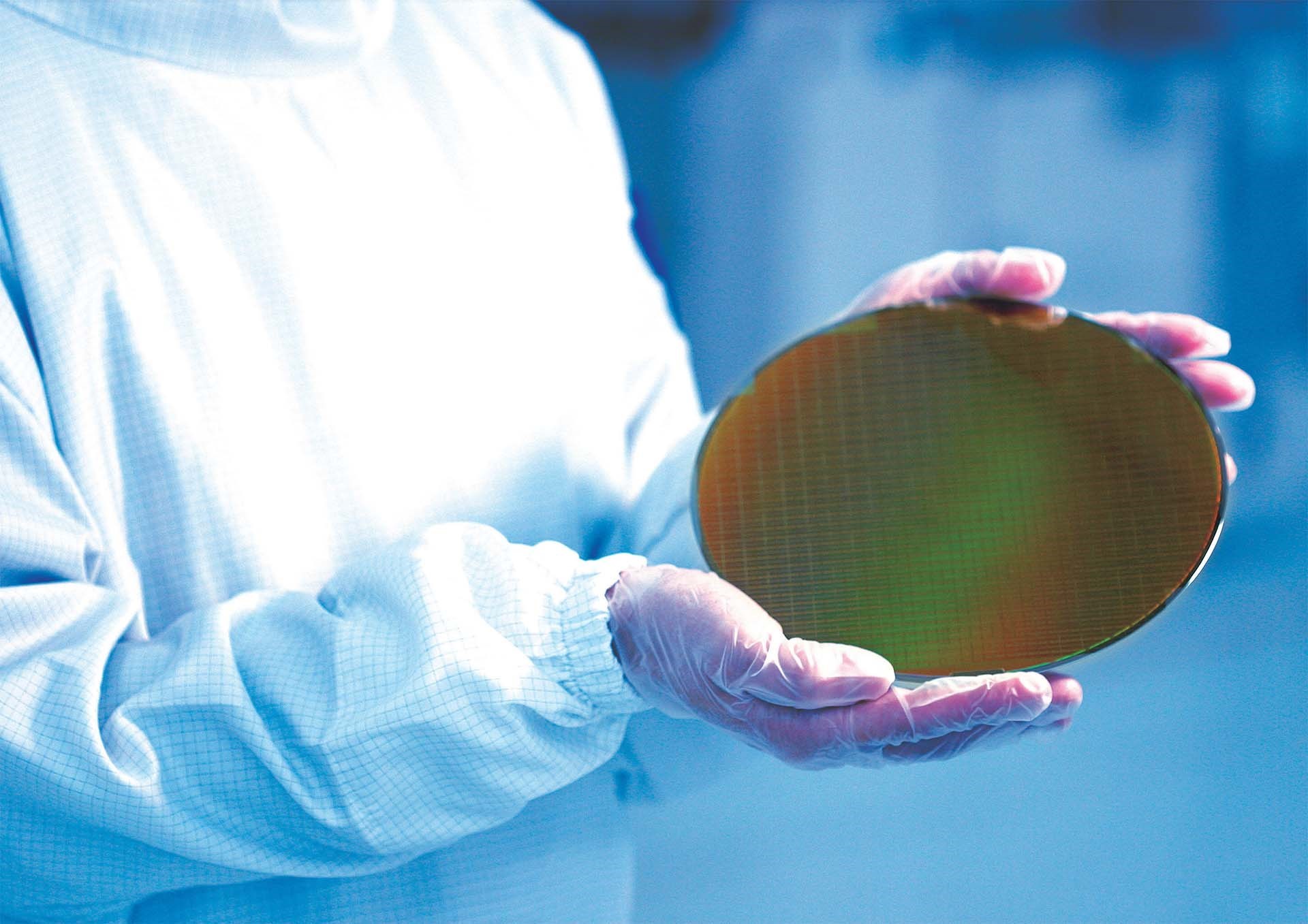
A report published a few months ago claimed that the efficiency of TSMC’s first-generation 3nm process (N3B) was 55% and that a wafer containing multiple chips cost $20,000. Efficiency means defect-free chips coming off this wafer. Often chip manufacturers charge their customers regardless of throughput.
TSMC is reportedly producing 60,000 to 70,000 wafers per month using the 3nm process, and that number is expected to rise to 100,000 wafers by the end of next year. Currently, 5% of the company’s revenues come from the 3nm process, but this rate is expected to increase to 10% next year.
 Samsung Foundry, on the other hand, hopes to change its image and beat TSMC by 2030 with advanced technologies. Samsung is using a new transistor design called GAA (Gate All Around), which is said to be more power efficient than the FinFET used by TSMC in the 3nm process. However, the company has still not been able to secure a major customer. It is rumored that AMD and Qualcomm may use Samsung’s next-generation 3nm and 4nm processes to produce some of their chips in the near future, but there is nothing concrete about this yet.
System LSI (Samsung’s chip design arm) is said to be developing a brand new Exynos 2500 processor that is said to be much more efficient than previous Exynos chips. In fact, it’s often referred to as the company’s “Dream Chip” and could be the first complex chip to be made using Samsung Foundry’s second-generation 3nm (3GAP) process.