 Semiconductors have become more important than ever before. As the undisputed leader of the industry in terms of production in this field, TSMC continues to stay ahead of its competitors in terms of performance and efficiency. On the other hand, Samsung, TSMC’s strongest and biggest competitor, will soon introduce more advanced production processes.
According to the statements, Samsung Foundry will introduce its advanced 3nm and 4nm chip manufacturing processes at the VLSI Symposium 2023 in June. The event will be held in Kyoto, Japan from 11-16 June 2023. During the chip industry event, the South Korean chipmaker will detail its second-generation 3nm and fourth-generation 4nm processes.
Samsung moves to next-gen 3nm and 4nm processes
 Both new processes are important to Samsung Foundry as they will help them gain more customers. As it will be remembered, it was criticized for not being as efficient as Samsung’s 4nm process and TSMC’s 4nm process. But chips manufactured using Samsung Foundry’s new SF3 (3nm GAP) and SF4X (4nm EUV) processes will bring better performance and efficiency.
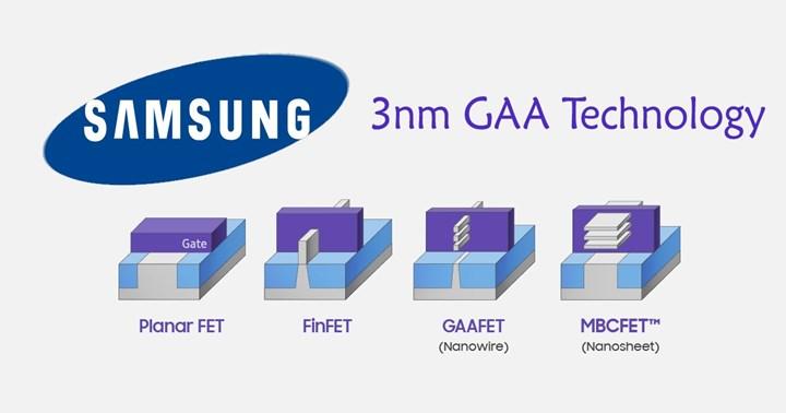
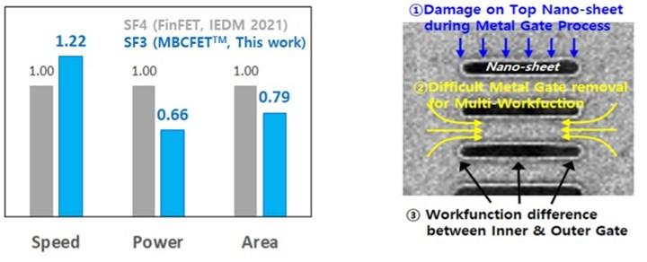
Samsung Foundry’s SF3 chip manufacturing process will use 3nm GAP technology. The new process is based on an improved GAA (Gate All Around) transistor, which Samsung calls MBCFET (Multi-Bridge-Channel Field-Effect Transistors). Compared to the SF4 (4nm EUV LPP), the SF3 is said to be 22 percent faster at the same power, or 34 percent more efficient at the same clock speeds and transistor count. In addition, a 21 percent smaller area is offered in terms of dice area. Meanwhile, for years it was said that one of the primary advantages of the GAA process was varying nanosheet channel widths in the same cell types. Samsung Foundry says the SF3 process will support it. So it can be deduced from here that SF3E (first generation 3nm process) does not fully support this.
Available for Exynos 2500 and Snapdragon 8 Gen 4
 Generally, Samsung’s first-generation chip manufacturing processes are not widely used, while subsequent generations are used by various chip companies. Judging by Samsung Foundry’s track record, we can expect the second-generation 3nm chip fabrication technology to be used by at least one major chip customer. Additionally, some rumors claim that Exynos 2500 and Snapdragon 8 Gen 4 can use the SF3 process.
Meanwhile, the South Korean firm’s fourth-generation 4nm process, designed to be used for high-performance computing applications such as server CPUs and GPUs, offers a 10 percent performance increase and 23 percent improved power efficiency compared to SF4 (second generation 4nm). This new process will compete with TSMC’s N4P (second generation 4nm) and N4X (third generation 4nm) nodes, which will be available in 2024 and 2025 respectively.