
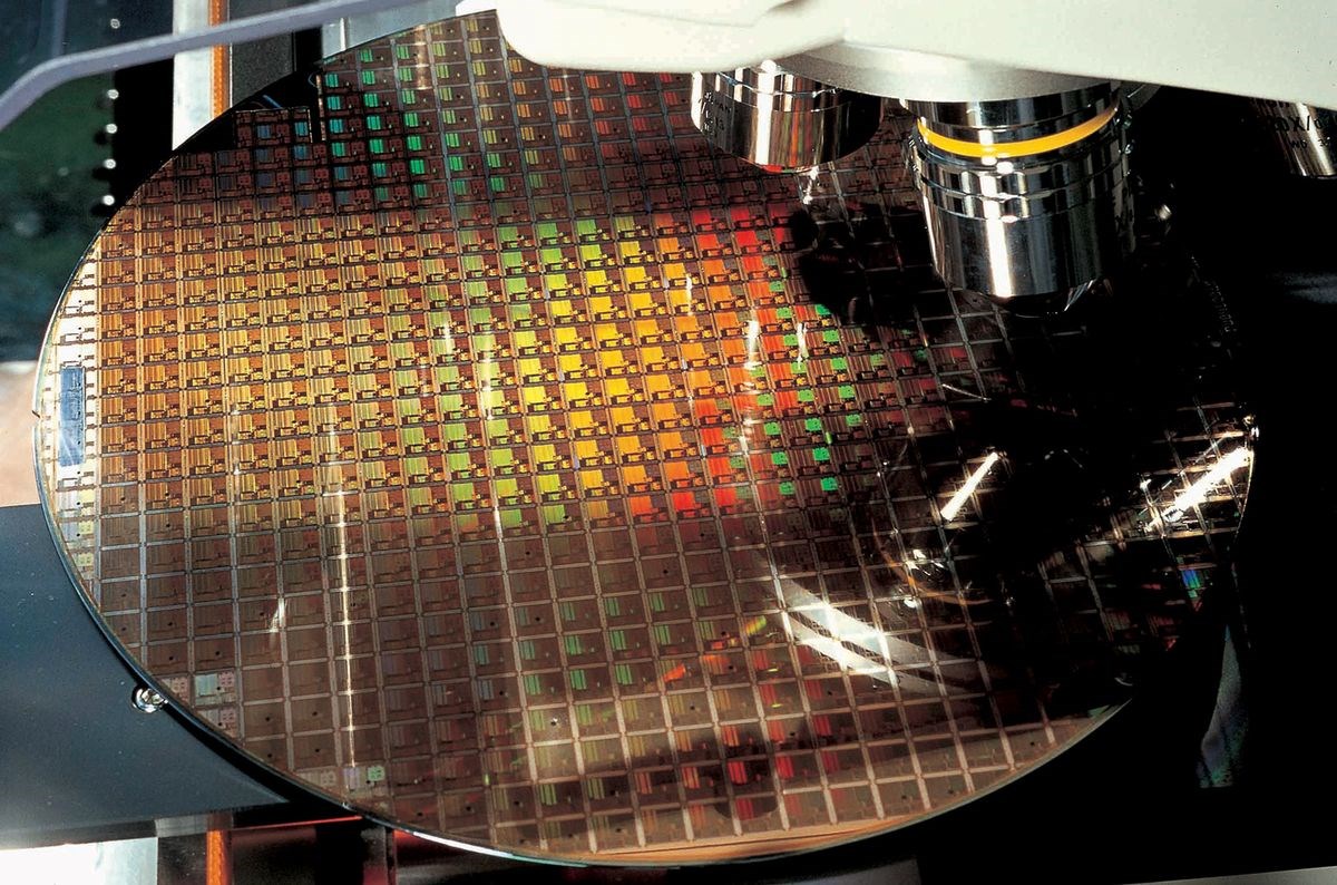
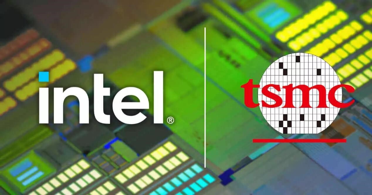
 One of the biggest competitions in the semiconductor world is in production technologies. Intel’s 18a (1.8nm class) and TSMC’s N2 (2nm class) production processes stand out as the most advanced production technologies of the industry. According to data released by Techinsights and Semiwiki, Intel’s 18A process offers higher performance, while TSMC’s N2 technology stands out with a higher transistor density.
Competition in semiconductors will be hot
According to the analysis of Techinsights, the N2 process of the TSMC reaches a level of 313 million transistors/mm² in high -intensity standard cell transistor density. On the other hand, Intel’s 18a process is 238 mTR/mm² and Samsung’s SF2/SF3P process is 231 mt/mm². However, there are some points to be considered here.
 First of all, high -density cells alone are not sufficient. Modern high -performance processors are not only based on them, but also a balanced structure using high performance and low power consumption cells. TSMC’s Finflex and Nanoflex technologies also contribute to this diversity.
Another issue is how Intel and TSMC’s high -performance and power -consumption standard cells are compared. Yes, TSMC may be ahead of the density side, but the difference may be smaller in other areas. Finally, the technical data offered by the companies are determined by the internal tests of the manufacturers. Performances may vary in real world conditions.
Intel 18A can have performance advantage
Nevertheless, Techinsights believes that when it comes to performance, Intel18A will be superior to TSMC’s N2 and Samsung’s SF2 (formerly SF3P). In addition, the Intel 18A process supports Powervia technology. Powervia can increase both performance and transistor density by providing power distribution under the transistors. TSMC’s N2 process does not have this feature. However, this does not mean that every 18a chips will use Powervia.
In terms of energy efficiency, Techinsights analysts predict that a chip produced by the N2 process of TSMC will consume less power than a similar chip produced by the SF2 process. In recent years, TSMC has shown significant leadership in low power consumption. Although it is unclear how Intel will perform in this regard, the 18A process is expected to provide power efficiency advantage in at least certain scenarios.
When we look at the production calendars, Intel 18A is scheduled to enter mass production in the middle of 2025. The first 18A -based processors will have “Panther Lake” chips and will be released at the end of this year. On the other hand, it is expected that high -volume production for the N2 process of TSMC will begin in the last quarter of 2025 and the first products produced with this process will not be released until the middle of 2026. Although there is no definite information on when Samsung’s SF2 process will enter production, the company states that it can start production in 2025.


