
 Chinese researchers have discovered the main source of defect in the production of Gallium Nitrür (GAN), the third generation semiconductor material that could revolutionize in advanced electronics. This development, which is especially critical for military practices, can increase China’s global competitiveness in the field of technology.
The reason behind the defects in GAN production
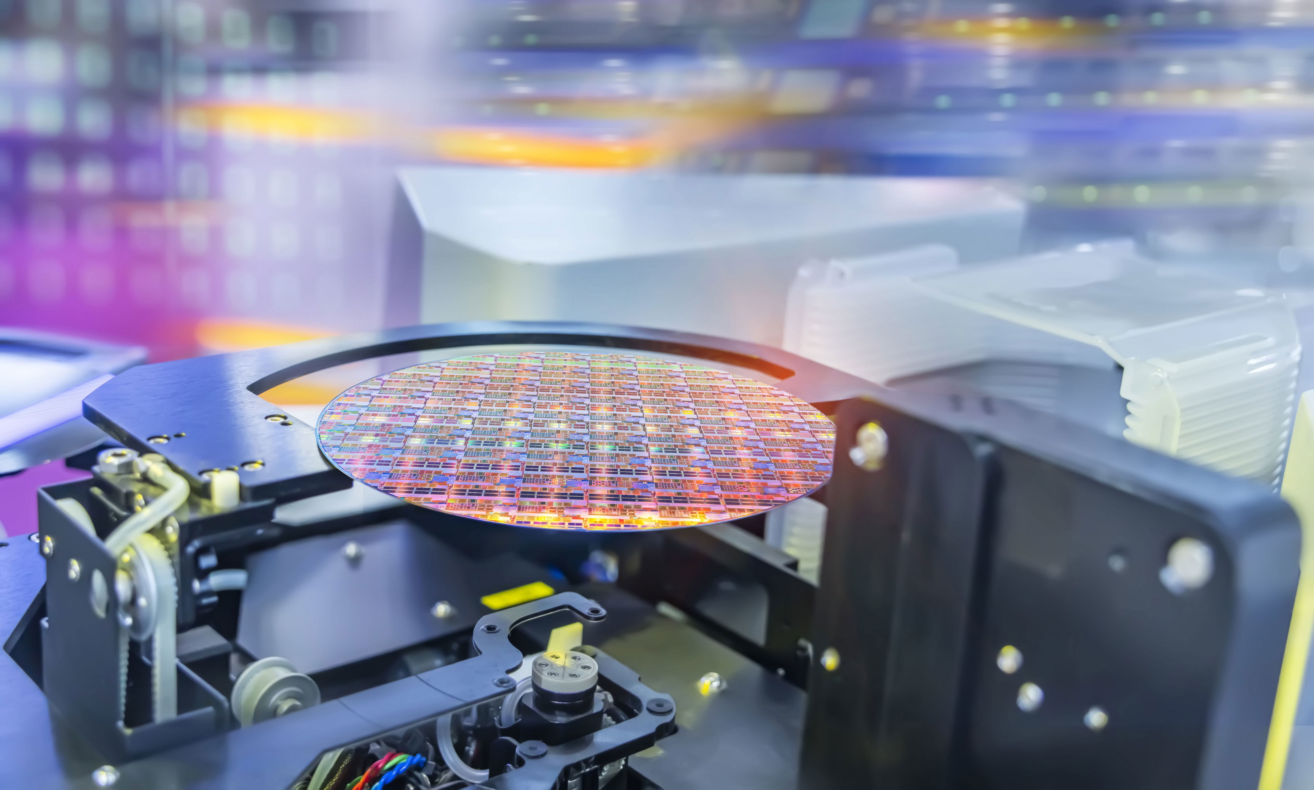
The team, led by Professor Huang Bing of Beijing University, identified the main cause of defects during Gan crystal growth. They found that the problem was caused by displacement defects that disrupt the crystal structure, leakage and low performance. The team found these flaws because Gan had a hexagonal atomic structure, which makes it different from the cubic structure of the silicone.
 In silicone -based semiconductors, defects can often be controlled by the “gliding” movement, while the defects in GAN were largely discovered from a process of changes in the number of atoms, which are largely called “climbing” (climbing). This process has not been fully understood in the industry so far.
The research team used the scanning-passing electron microscope (STEM) technology to detect atomic-scale defects. The team discovered that they can control the formation of imperfections with a method called “Fermi level setting”. By changing the energy levels of the electrons, they managed to minimize structural defects in GAN crystal.
Professor Huang Bing said, “Traditional defect reduction methods are often used superficial solutions such as using different substrates or adjusting crystallization temperatures. However, these approaches only deal with symptoms, not the reason. ”
Why is Gan important?
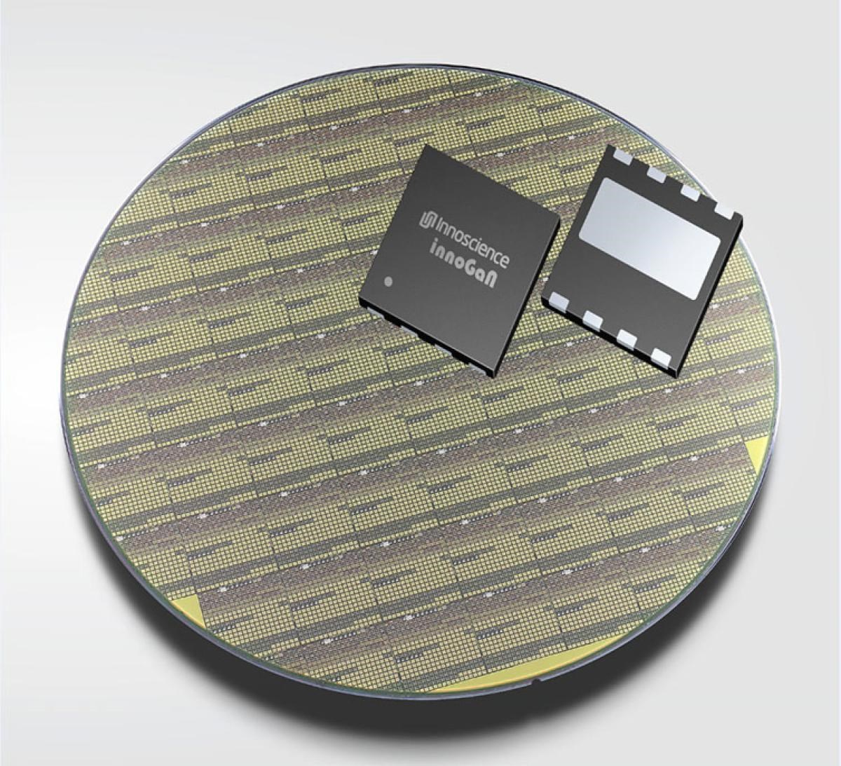
GAN is widely used in 5G base stations, radar systems, military communication, aviation and electronic warfare systems. The ability to operate in high voltage, frequency and temperature conditions makes it a preferred material instead of silicone.
Great powers like the USA are largely dependent on GAN technology in advanced chip production. However, China controls approximately 98 %of global gallium production and recently banned exports of this element. This increased costs by making it difficult for the US (especially the Pentagon) to supply cost -effective GAN chips.


