
 Scientists have developed a new abrasion technique that can revolutionize the production of 3D Nand Flash memory. This method of hydrogen fluoride plasma -based method may increase the data storage intensity by doubleing the abrasion rate during the chip production process.
In semiconductor production for those who do not know, the erosion (etching) is the process of creating circuit patterns by removing unwanted materials from certain layers in a controlled manner. This process creates the sensitive structure of the microcheps by selecting the material other than the areas determined by photolithography. Abrasion is usually performed by wet (chemical solutions) or dry (plasma -based) methods. Dry abrasion is widely preferred in modern semiconductor production that requires high sensitivity and vertical profiles.
More storage for smaller areas
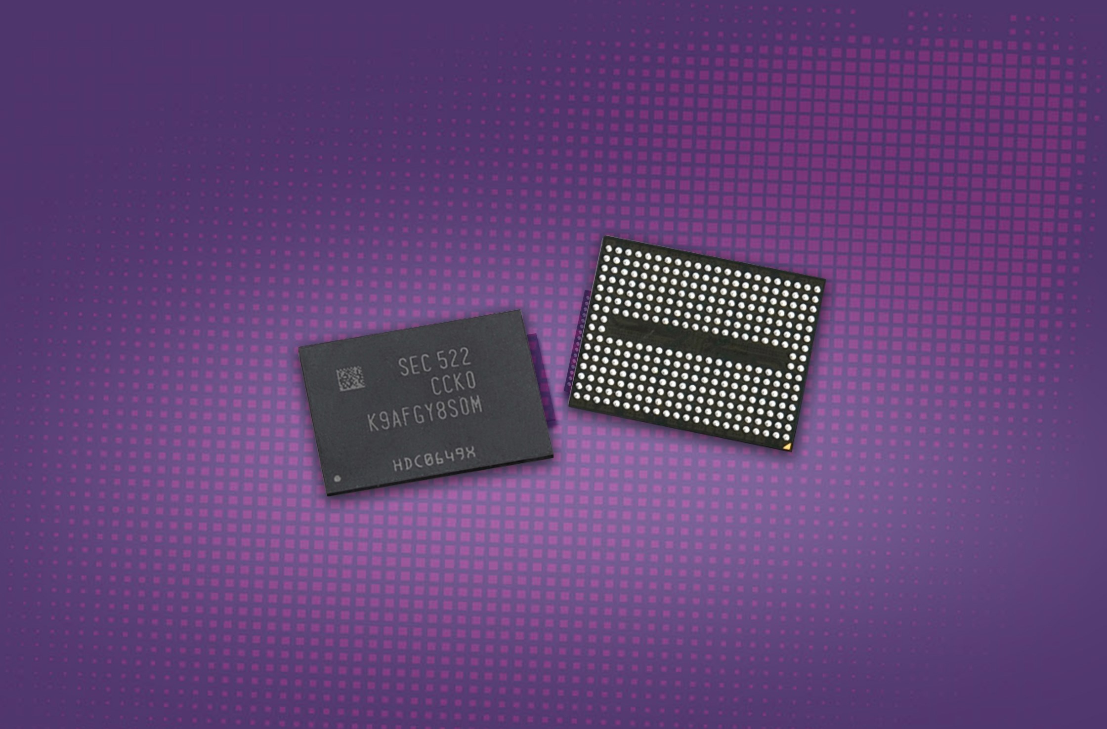
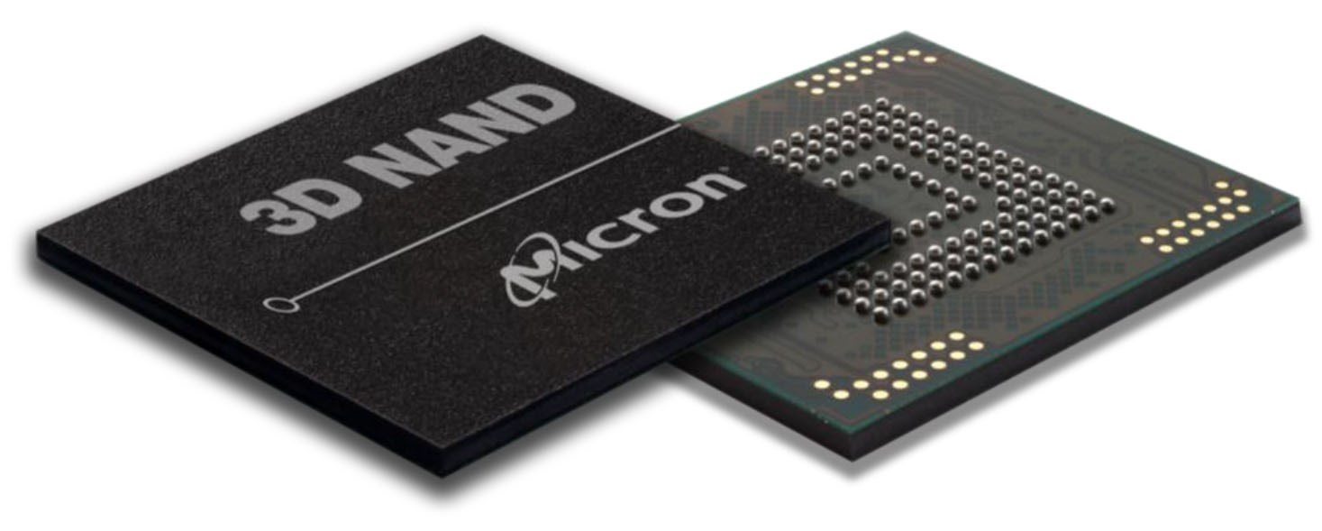
Nand flash memories, which are used on many devices from USB memory to smartphones, switched to the vertical stacking method called 3D Nand to increase data storage capacity. Today, giants such as Micron, SK Hynix and Samsung work on 400 -layer memory chips, while the increasing number of layers makes the production process more complex.
 One of the most challenging of these is the abrasion process. During production, silicone oxide and silicone nitride layers need to be drilled with millimeters with millimeters. Researchers from Lam Research, Colorado Boulder University and Princeton Plasma Physics Laboratory managed to use cryogenic (low temperature) hydrogen fluoride plasma to accelerate the wear process. With the new method, the abrasion rate was increased from 310 nanometters to 640 nanometers per minute. Moreover, it was observed that the holes opened were cleaner. The team tried to add new components to the hydrogen fluoride plasma to further improve this method. Phosphorus trifloride has increased the silicone dioxide abrasion rate to four times.
It remains unclear when the new method can be integrated into commercial production. Igor Kaganovich of Princeton Plasma Physics Laboratory emphasizes that the need for more intensive memory technologies increased in artificial intelligence and large data age, and that this method may overcome a significant production obstacle. It’s too early to tell you if it will result in cheaper or more dense nand chips for consumers. The commercial applicability of the technique needs to be proved and scaled for mass production.


